 简体中文
简体中文 English
 Español
Don't hesitate to send a message
Search
Recent Post
Newsletter
The prominent large-scale electronic switching system was the number
In telecommunications, an electronic switching system (ESS) is a telephone switch that uses digital electronics and computerized control to interconnect telephone circuits for the purpose of establishing telephone calls. The generations of telephone switches before the advent of electronic switching in the 1950s used purely electro-mechanical relay systems and analog voice paths. These early machines typically utilized the step-by-step technique. The first generation of electronic switching systems in the 1960s was not entirely digital in nature but used reed relay-operated metallic paths or crossbar switches operated by stored program control (SPC) systems. Announced in 1955, the customer trial installation of an all-electronic central office commenced in Morris, Illinois in November 1960 by Bell Laboratories.[1] The first prominent large-scale electronic switching system was the Number One Electronic Switching System (1ESS) of the Bell System in the United States, introduced in Succasunna, New Jersey, in May 1965. Later electronic switching systems implemented the digital representation of the electrical audio signals on subscriber loops by digitizing the analog signals and processing the resulting data for transmission between central offices. Time-division multiplexing (TDM) technology permitted the simultaneous transmission of multiple telephone calls on a single wire connection between central offices or other electronic switches, resulting in dramatic capacity improvements of the telephone network. With the advances of digital electronics starting in the 1960s telephone switches employed semiconductor device components in increasing measure. In the late 20th century telephone exchanges without TDM processing were eliminated and the term electronic switching system became largely a historical distinction for the older SPC systems. Optical packet switch systems with fiber delay line (FDL) buffers provide high-throughput, bit-rate independent, energy-efficient, and transparent forwarding. However, the FDL buffer experiences scalability issues and, thus, cannot accommodate a large amount of network traffic. In this paper, we have studied the network performance of the FDL buffer. Due to the discrete-time nature of the FDL buffer, the throughput of Transmission Control Protocol (TCP) applications is not improved drastically in spite of the addition of extra FDLs.
Then, we propose optical and electronic combined buffer architecture. The combined buffer is composed of an FDL buffer and a supplementary electronic buffer having power management functions according to its occupancy. The combined buffer uses only the FDL buffer and keeps its energy efficiency when traffic volume is low. In doing so, this architecture reduces power consumption to 70% of that of a buffer composed only of electronic devices under non-peak traffic. As the traffic volume increases, the combined buffer turns on its electronic devices and accommodates the increased traffic. Simulation results reveal that the proposed buffer architecture obtains 1.5 times larger throughput than that of the existing FDL buffer against suddenly increased traffic. Finally, we show that the supplementary electronic components have to be ready to use in less than 300 ms. Here we demonstrate that we can rationally and finely control the functionality of different DNA-based nanodevices and nanoswitches using electronic inputs. To demonstrate the versatility of our approach we have used here three different model DNA-based nanoswitches triggered by heavy metals and specific DNA sequences and a copper-responsive DNAzyme. To achieve electronic-induced control of these DNA-based nanodevices we have applied different voltage potentials at the surface of an electrode chip. The applied potential promotes an electron-transfer reaction that releases from the electrode surface a molecular input that ultimately triggers the DNA-based nanodevice. The use of electronic inputs as a way to finely activate DNA-based nanodevices appears particularly promising to expand the available toolbox in the field of DNA nanotechnology and to achieve a better hierarchical control of these platforms.
The growing and exciting field of DNA nanotechnology, where synthetic nucleic acids are rationally engineered and designed to build novel responsive nanomachines or functional nanodevices, represents one of the interesting examples of bio-inspired technologies.1 The majority of these DNA-based nanodevices rely on a common basic mechanism: a target molecular input is recognized by a DNA probe sequence and the binding event is coupled to a mechanical motion or an output signal.2 Even the complex functional DNA-based nanostructures (i.e. origami) are thus based on the use of relatively short DNA sequences (or nanoswitches) that in the presence of a specific molecular input undergo binding-induced conformational changes or DNA-based reaction and, by doing so, confer to the nanostructure an useful function.3,4 Despite the advancements achieved in this field, the need to have a better control of such nanodevices remains still partially unmet. To fully exploit these platforms it would thus be crucial to find new strategies to trigger and activate their function in a highly controllable fashion.Since the revolutionary discoveries of Volta, Faraday and other pioneer electrochemists,5 the possibility to control redox reactions through an electronic input (applied voltage) has represented one of the major breakthrough in the history of chemistry.
It is now more than 200 years that electrochemistry has been applied for a wide range of applications from energy production6 to industrial manufacturing7 and sensing.8 Because of the low cost of instrumentation, possible miniaturization and high level of control, electrochemistry might also represent an interesting opportunity for novel bio-technological applications. Redox reactions are in fact routinely used in Nature to activate, regulate and control a wide range of biological pathways and reactions (such as photosynthesis and energy storage/release).9 In a similar way, electrochemistry could thus be applied to modulate bio-inspired tools and devices.10–13 Despite this, the possibility to use electronic inputs to control DNA-based nanodevices has seen very little application to date.14Motivated by the above arguments, here we propose an approach to electronically control a wide range of DNA-based nanodevices. We did so by controlling, through an electronic input, electron transfer across an electrode-solution interface thus promoting redox reactions in a highly controllable fashion. More specifically, as the electronic input we used here a voltage potential applied at the surface of an electrode chip. Such applied potential promotes an electron-transfer reaction at the electrode-solution interphase to the release of a molecular input that ultimately triggers a DNA-based nanodevice in solution (Fig. 1). To demonstrate the versatility of our approach we have used here four different model DNA-based nanodevices or nanoswitches that can be activated by different molecular inputs.
https://www.monroswitch.com/
OUR PRODUCTS
Recommended Products
-
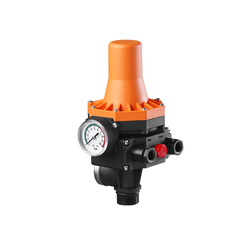
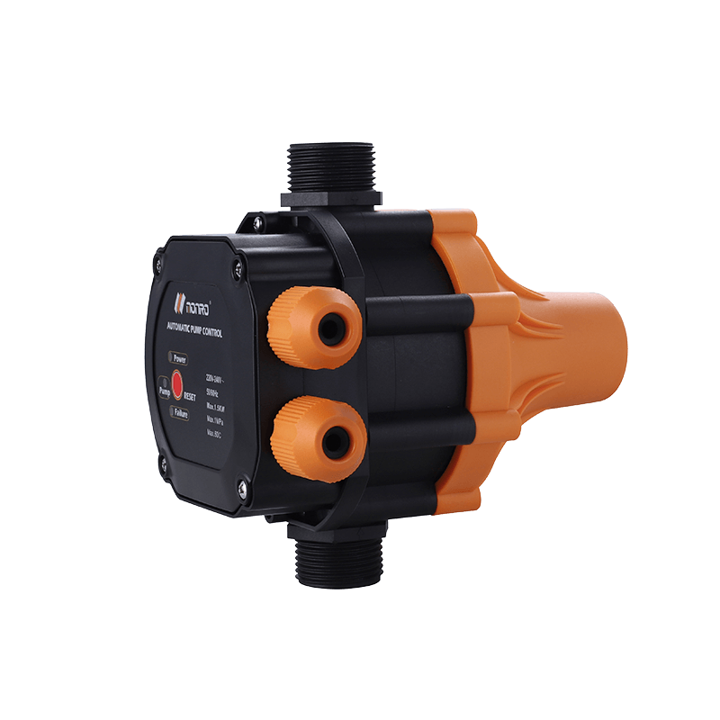
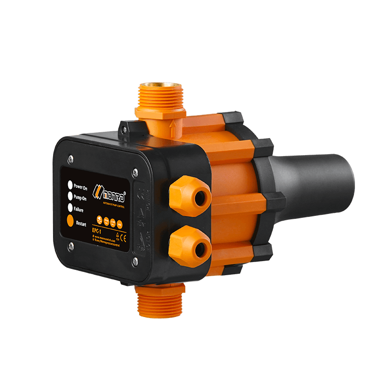 EPC-1
EPC-1Monro EPC-1 model pump controller is the classic and basic type, was loved by user in the global mar...
-
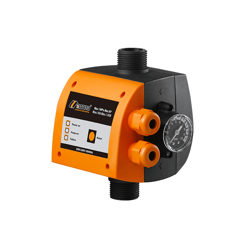
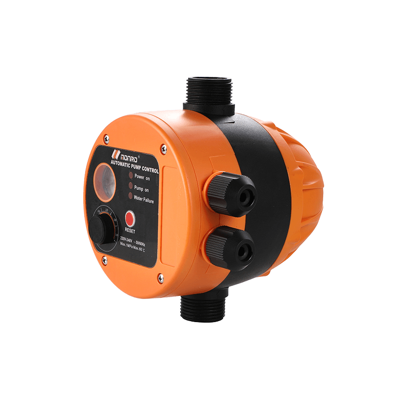
 EPC-3
EPC-3Monro EPC-3 spain design auto on and off press control, an intelligent and economical system designe...
-
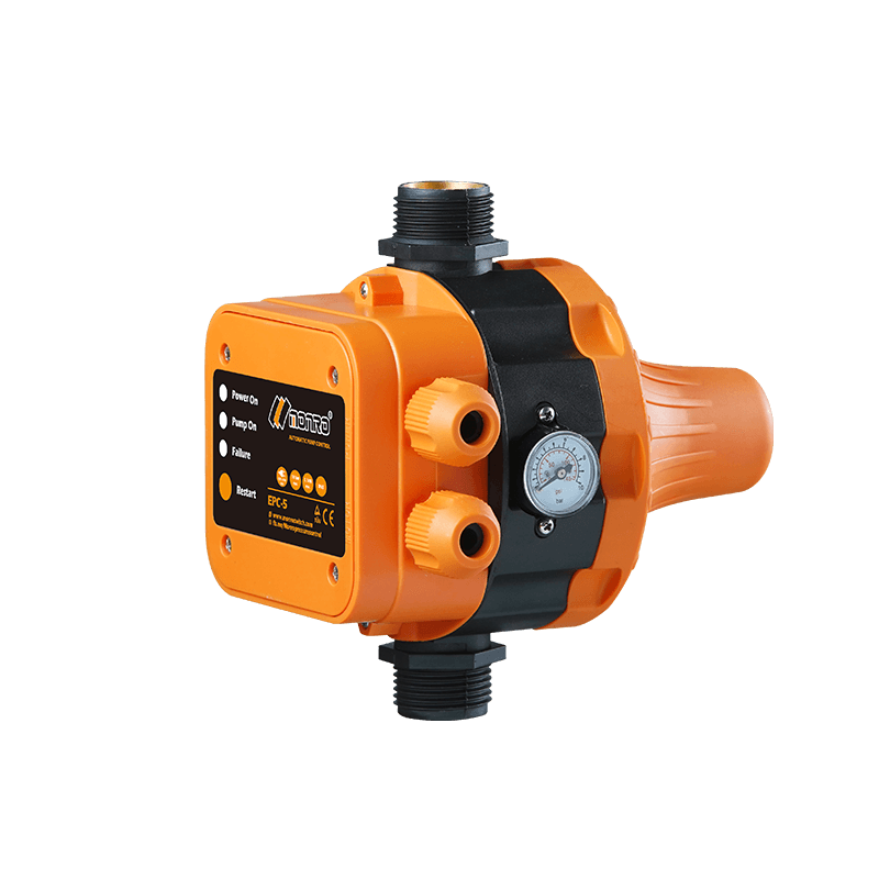 EPC-5
EPC-5Monro EPC-5 model automatic pump control, a device which assembled on the water pump (recommended si...
-
 EPC-9
EPC-9Monro EPC-9 model pressure controller, is a big power device for automatic control and protection of...
-
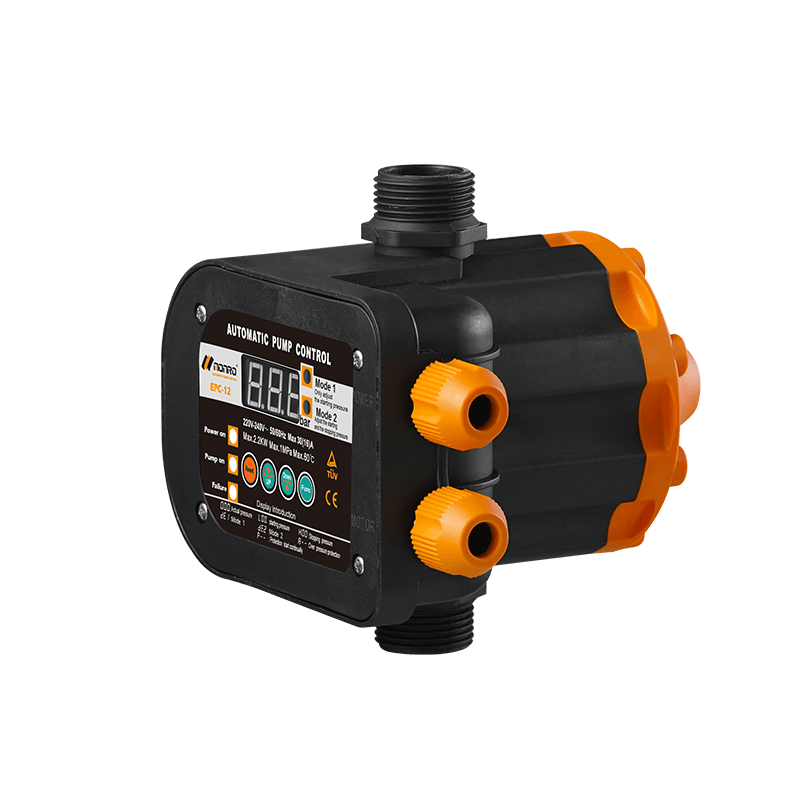 EPC-12
Monro EPC-12 smart top-level automatic pump control is a multi-function model combined with traditio...
-
 EPC-14
Monro EPC-14 model pressure control is a big power device for automatic control and protection of el...
-
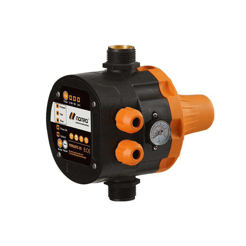 EPC-15
Monro EPC-15 model automatic pump control, a device which assembled on the water pump (recommended s...
-
 EPC-16
EPC-16 is the new patent pump controller by Monro. Its key highlight is tooless (manual knob) start...
contact us
find our office
find our office
Committed to providing professional pressure control solutions for various types of water pumps and air compressors.
Mobile
 Wechat
Copyright © 2024 Zhejiang Monro M&E Co., Ltd. All Rights Reserved.
Wholesale Pressure Control Switch Manufacturer
